Research
The Garno group is working to develop SPM measurements with hybrid instrument configurations which can be applied for chemistry studies at the molecular-level. Along with high resolution images, maps of surface forces (e.g. magnetic, electrostatic, elastic, etc.) can be acquired concurrently with topography images to achieve unprecedented sensitivity. Macroscopic measurements of optical and electronic material properties do not scale with size at the nanometer level. New phenomena found in materials such as quantum dots, superparamagnetic nanoparticles, and SERS substrates are all attributable to size-dependent phenomena – which can be studied with SPM instruments.
One may think that scanning probe microscopy (SPM) instruments are mainly used to "look" at a surface, such as with an optical microscope, however SPM studies encompass dozens of measurement and lithography modes for fundamental studies in Chemistry and other disciplines. The atomic force microscopy (AFM) has three main capabilities: surface force measurements, nanoscale imaging at the atomic or molecular level, and molecular manipulation (nanoscale lithography).
Work in Dr. Garno's laboratory is multidisciplinary. Applications of scanning probe microscopy (SPM) instruments cover a broad range of scientific disciplines: electrochemistry, polymers, organic thin films, nanoscale lithography, life sciences, material science and physical measurements. Garno has collaborated with research groups throughout LSU and at other campuses, and will continue to provide resources and expertise – with the main requirement that the studies require characterizations and measurements at the nanoscale.
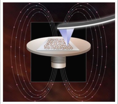
Concept of magnetic sample modulation AFM.
Our group has developed a hybrid instrument configuration using magnetic sample modulation (MSM) for studies of magnetic nanomaterials. A soft, nonmagnetic cantilever that is operated in contact mode is used to detect the physical motion of samples which are driven to vibrate by an external electromagnetic field. A non-coated commercial atomic force microscopy (AFM) probe can be used for MSM which enables high resolution imaging of very small features. The tip is operated in continuous contact with the surface. An AC voltage is applied to a solenoid located under the sample to generate a magnetic field which alternates in polarity, frequency, and strength to precisely drive the actuation of the sample. The periodic motion of the vibrating sample can be tracked by changes in the deflection of the tip. The changes in phase angle and amplitude as the tip interacts with the vibrating sample are plotted as a function of tip position to produce MSM phase and amplitude images. Frequency spectra of the nanomaterials in response to an applied magnetic field also can be acquired with MSM by placing the AFM tip in direct contact with a vibrating nanostructure and sweeping the field frequency.
Characterizations of local electronic and photoelectric properties of nanomaterials has become important for developing new technologies and energy efficient materials. Particularly for emerging international efforts to develop organic photovoltaic (OPV) surfaces for solar cells, new instrumental tools are needed for characterizing photonic properties of materials such as conductive polymers, organic thin films or molecular layers. The spatial constraints of the distance and proximity of donor and acceptor components within the interfacial junction of OPV cells dictate the efficiency of energy conversion. We are developing an instrument configuration for local SPM measurements of photocurrents, to map changes in the induced photocurrents versus the conductance of patterned samples of designed polythiophenes, porphyrins and phthalocyanines.
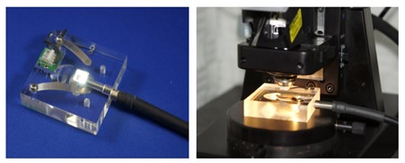
A fiber optic cable is used to direct light to the sample for AFM measurements of photocurrent.
We have designed an integrated instrument platform using the established SPM mode of current-sensing atomic force microscopy (AFM) by modifying the sample stage. Light can be introduced to samples with selected wavelengths of irradiation. Rather than use the sample bias voltage to induce a current, light will be used to generate photocurrents that can be sensitively measured by conductive probe AFM.