Electrochemical Engineering and Semiconductors Research at LSU
Electrochemical reduction of CO2
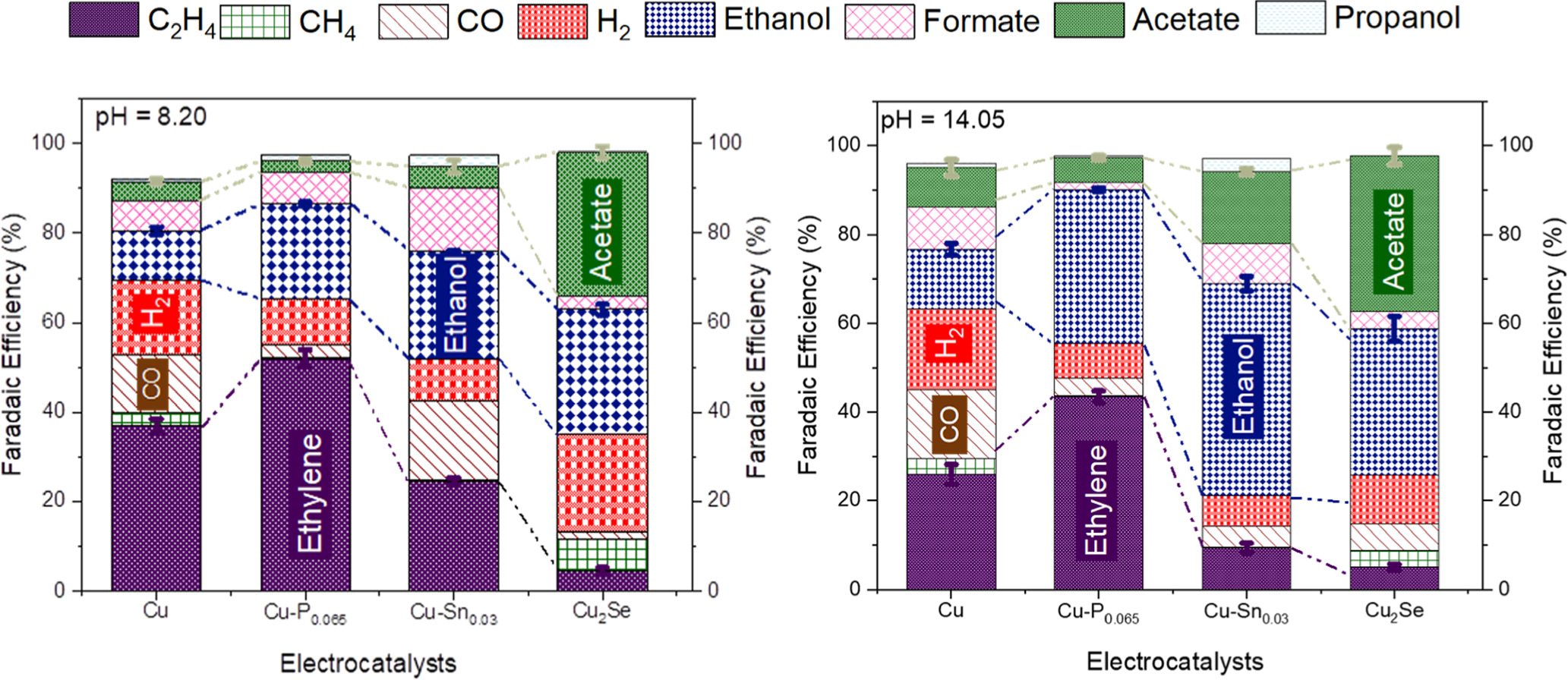
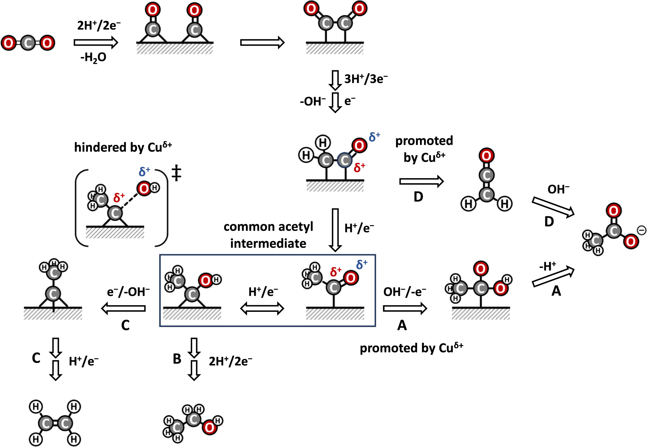
CO2 concentrations in the Earth’s atmosphere have been on a dramatic rise over the past century, resulting in an increase in temperature anomalies and deleterious climate change effects (global warming). As a result, developing sustainable technologies that can transform CO2 into value added chemicals provides a promising pathway to reduce the rising levels of CO2 emissions. Our group aims at providing electrochemical transformations of CO2 into value added chemicals especially into C2+ products including ethanol, ethylene and acetate. Electrochemical reduction of CO2 provides an opportunity to store renewable energy as fuels with much greater energy densities than batteries. Our aim is to improve the product selectivity (Faradaic efficiency), energetic efficiency and conversion rate (current density) through the development of suitable electrocatalysts, modification of the electrode surface and understanding the various transport mechanisms involved in the electrode membrane assembly. We as a group seek to yield C2+ products in considerable amounts and concentrations to push for the commercialization of the electrochemical carbon dioxide formation.

Semiconductors Research
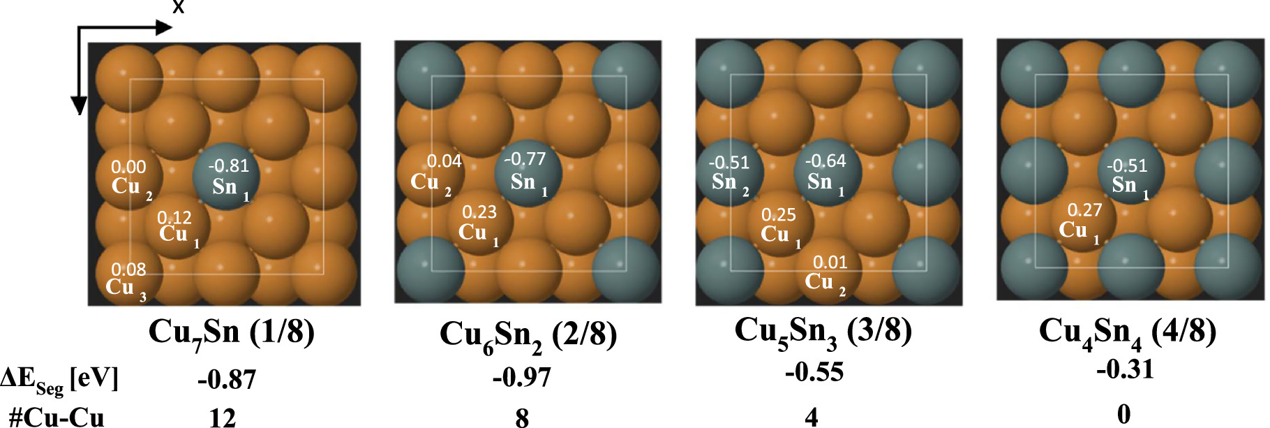
The study of copper-dielectric interfaces is critical in microelectronics, especially for the creation of integrated circuits (ICs). As device dimensions decrease and performance demands rise, understanding the interactions at the copper-dielectric interface becomes critical for enhancing reliability and functionality. Copper (Cu) is commonly utilized in ICs because of its ability to transmit higher currents with less resistance than aluminum. However, integrating copper with dielectric materials, which are used to insulate and isolate various circuit components, poses major hurdles. Adhesion, electrochemical migration, and the creation of interfacial layers are all challenges that can have an impact on electronic device performance and longevity. Our group seeks to understand the interfacial chemistry of copper in ensuring excellent dielectric behaviors for lasting performance.
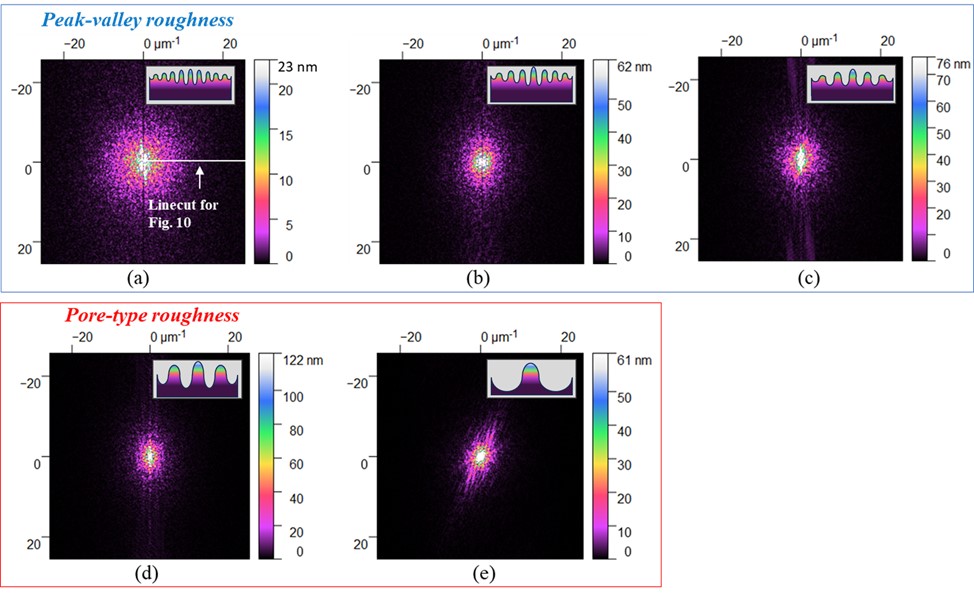 Two-dimensional Fast Fourier Transform (FFT)
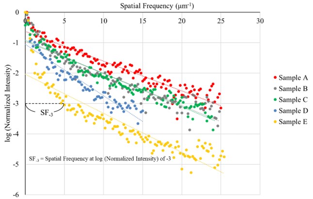
log (normalized intensity) after 2D FFT
DOI: 10.1109/TCPMT.2024.3399662/doi.org/10.1021/acsami.4c16414
